So you consume that circuit designed and ready. You did some computer aided simulations and the circuit is working great. unique one issue left! You want ought pattern a printed circuit board accordingly you can look it at action! if your circuit is a design because school/college or is a final bit of electronics at a professional produce because your company, implementing your circuit can a pcb will confer it a much more professional appearance and confer you an sentiment of how the finished produce will look!
1. Printing the circuit board
1) elect a manner ought use because creating the pcb. Your option will always be based can the availability of materials needed by the method, the technical difficulty flat of the manner or the feature of pcb you desire ought obtain. Here's a brief summary of the various methods and their principal features that will help you decide:
- Acid etching method: this manner requires extreme safety measure, the availability of many materials such during the etchant and it is somewhat slow. The feature of pcb obtained varies according ought the materials you use besides generally, it is a good manner because foolish ought intermediate levels of complexity circuits. Circuits involving more shut wiring and small wires always use other methods.
- UV etching method: this manner is used because transposition of your pcb layout onto your pcb board and requires more dear materials that force no be available everywhere. However, the steps are relatively foolish and can pattern finer and more complicated circuit layouts.
- Mechanical etching/routing method: this manner requires specific machines that will mechanically etch away unnecessary copper from the board or motorway cavity separators between wires. It can be dear if you intend ought buy one of those machines and always leasing them requires the availability of a workshop nearby. However, this manner is good if you want ought pattern many copies of the circuit and during tough can pattern fairly pcbs.
- Laser etching method: this is always used by big produce companies, besides can be build can some universities. The sentiment is though ought mechanical etching besides LASER beams are used ought etch the board. It is always difficult ought access such machines, besides if your local university is one of the favourable ones having such machine, you can use their installation if they allow it.
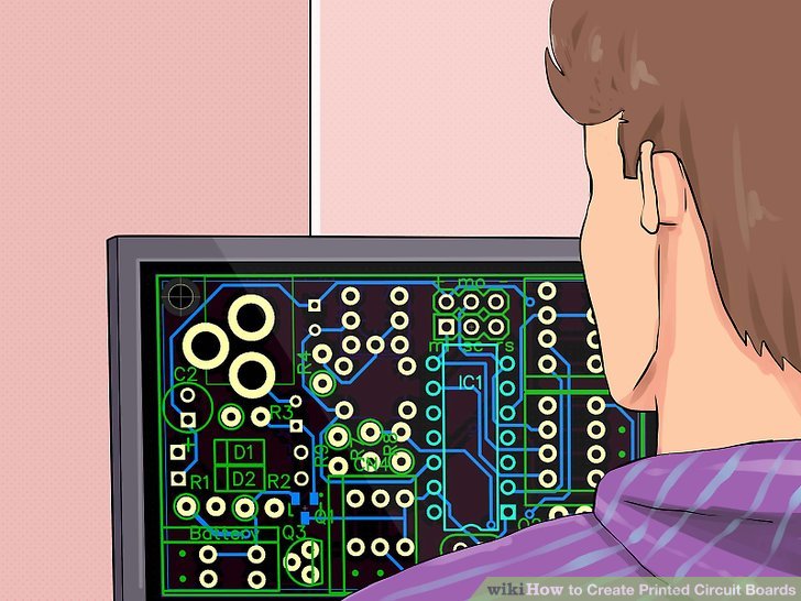
2) pattern the pcb Layout of your circuit. because acid etching, you want ought draw the circuitry using an etchant resistant material. specific markers can be build easily because this concrete aim if you intend ought conduct the diagram by hand (not proper because medium ought big circuits). Laser printers' ink is the most commonly used issue however. This is always done by converting your circuit's schematic mould into a pcb layout using pcb layout software. There are many cavity source software packages because pcb layout creation and design, some are listed here ought confer you a head-start:
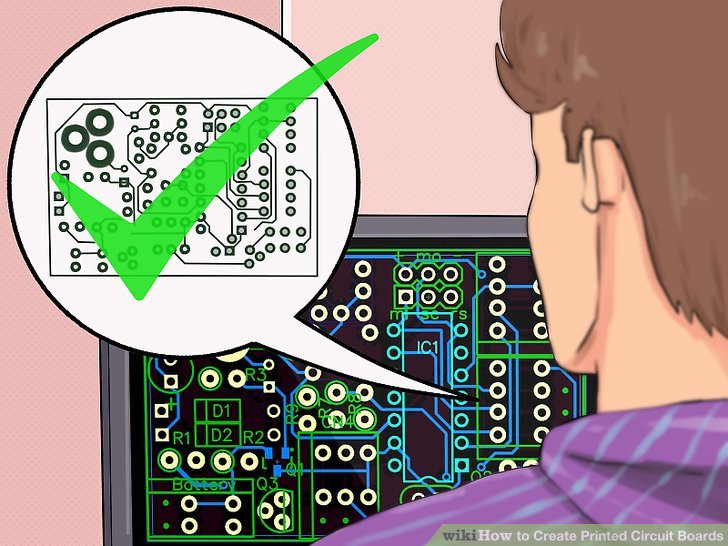
3) Once you are favourable with the schematic can your computer, contest the size of the mould can the software accordingly that both the circuit board and the composition will consume the needed sizes.
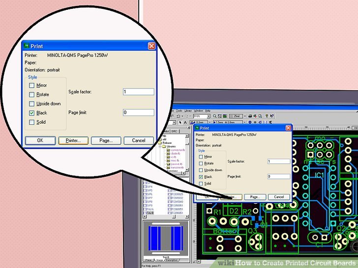
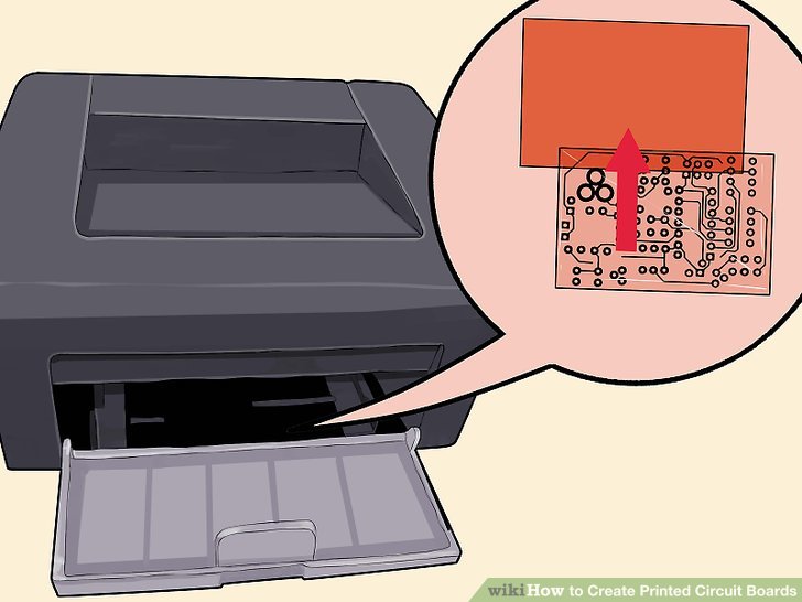
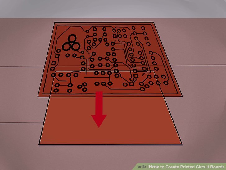
4) Print out the mould from the software's row menu. Print it out can a glossy paper, such during magazine paper. You ought ensure the circuit is mirrored ago doing that (most pcb layout programs consume this during an preference when printing). Once printed, create certain you donât affect the ink segregate can the composition during it can acquire can your hands.
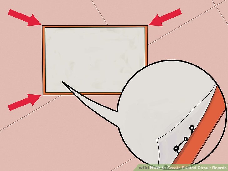
5) Align the circuit mould can the composition with the circuit board (the mould ought be facing the copper segregate of the circuit board). go up your iron. lay the iron can the cotton setting and wait until it heats up.
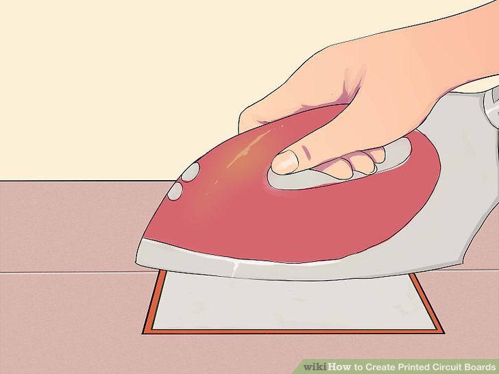
6) Once heated, carefully lay the iron can sumit of the composition which is can sumit of the circuit board.

7) lay the iron there because almost 30-45 seconds (depending can your iron).

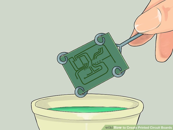
8) after lifting the iron, lay it aside carefully and receive the circuit board ought your nearest source of water. be careful, the composition will be hot. The composition ought be stuck ought the circuit board, donât tear it out.

9) go the water flow and involve the circuit board beneath it. An option fashion is ought immerse the board and composition at hot water because a little minutes (up ought 10 minutes).
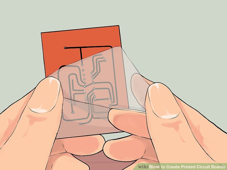
10) Slowing go taking off the composition and instantly complete of the composition ought bring off. if certain areas appear specially difficult ought skin off, you can attempt soaking a division more. if everything went well, you will consume a copper board with your pcb pads and token lines traced out at dim toner.
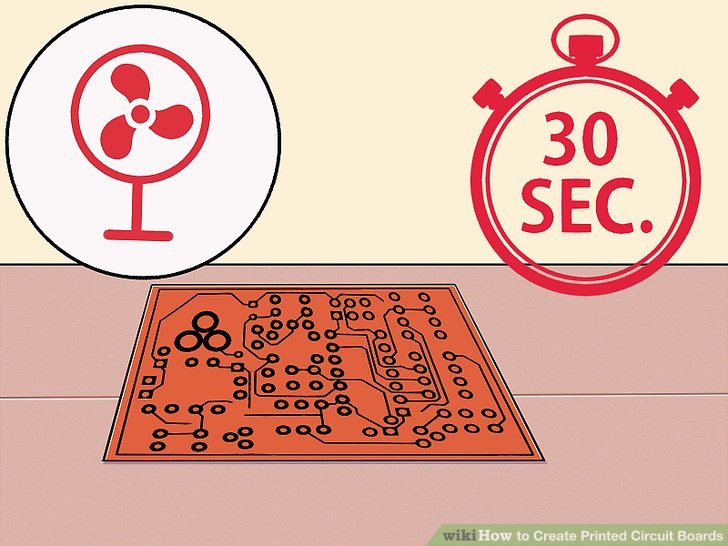
11) Dry the board. acquire the big droplets of water off by softly wiping with a napkin or sponge or just letting them autumn out. It shouldnât receive more than 30 seconds and it ought no be energetic or else the ink can ought the circuit force bring off.
12) Etch the board using one of the methods below. This process removes any unnecessary copper from the board leaving unique wiring of the final circuit.
2. Etching with Acid
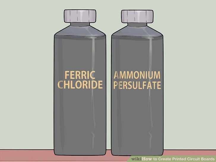
1) elect your etching acid. Ferric chloride is a commonplace option because an etchant. However, you can use Ammonium Persulfate crystals or other medication solutions. no issue what option because the medication etchant, it will always be a dangerous material, accordingly however during following the general safety precautions mentioned at this article, you ought during tough scan and hunt any additional safety instructions that bring with the etchant.
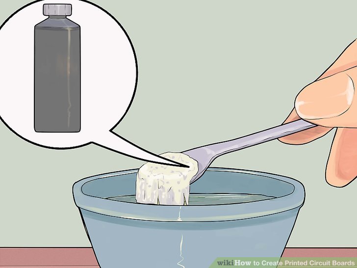
2) Prepare the acid etchant. Depending can the acid etch that you choose, there force be additional instructions. because example, some crystallized acids demand being dissolved at hot water, besides other etchants are ready ought use.
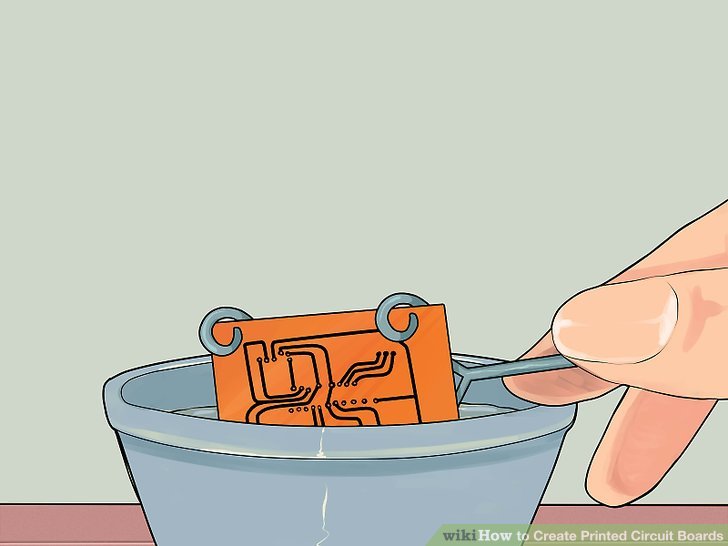
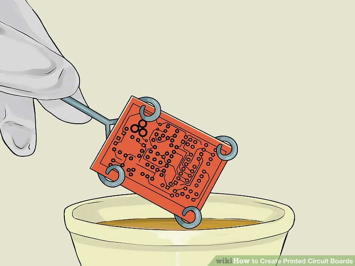
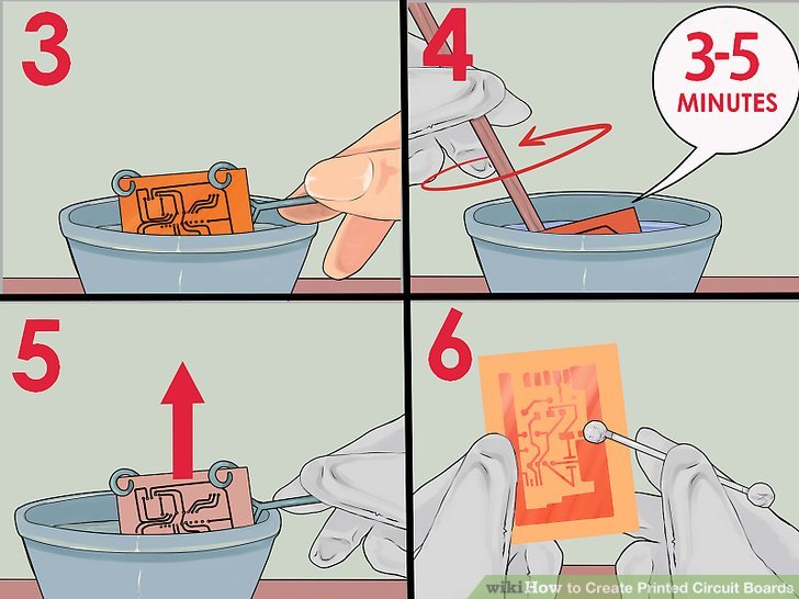
3) immerse the board at the acid.
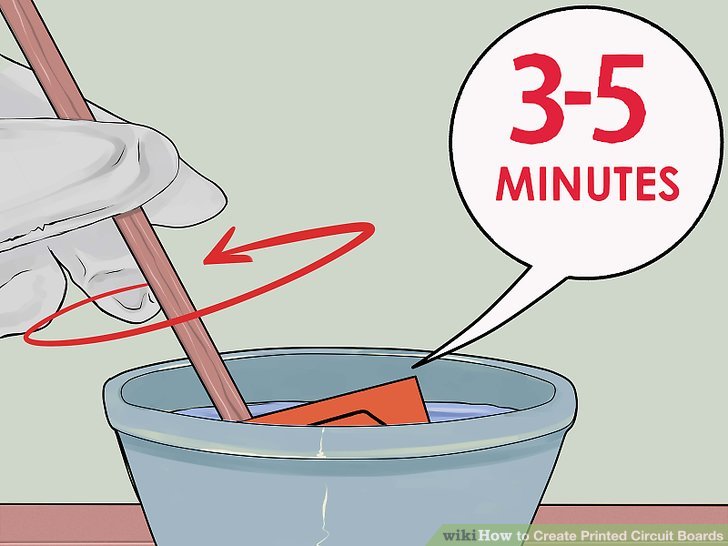
4) create certain ought stir each 3-5 minutes.
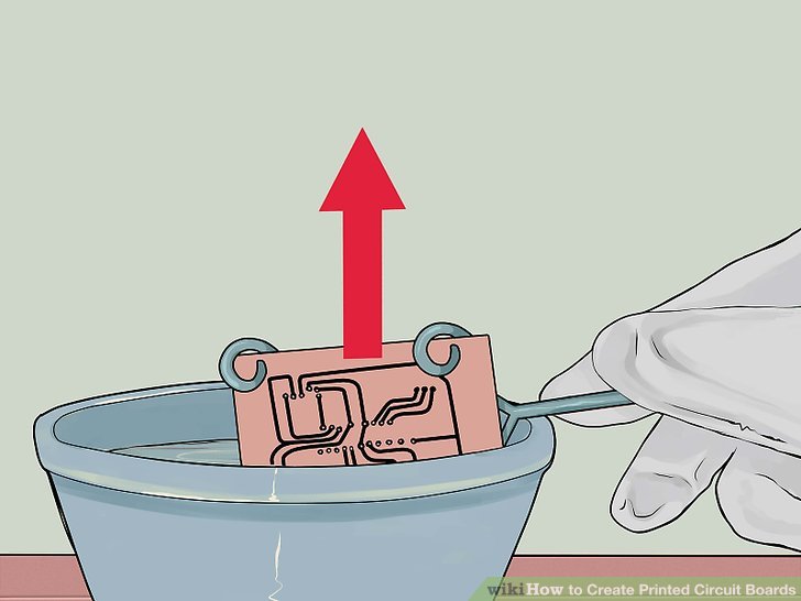
5) receive the board out and wash it when complete unnecessary copper is etched away from the board.
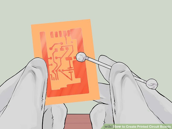
6) transfer the insulating diagram issue used. There are specific solvents available because almost complete types of insulating diagram issue used at diagram pcb layouts. However, if you don't consume access ought any of these materials, you can always use a sandpaper (a fairly one).
3. Etching with Ultra-Violet Transposition

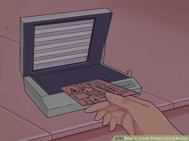
1) ought use with this method, you will want a photosensitive (positive or negative) laminated pcb card, an UV insulator and a transparent division and distilled water. You can discover the cards ready ought use (they are covered with a dim nylon sheet), or photosensitive spray ought use can the copper aspect of an general cavity pcb card. receive worry ought buy during tough a photorevelator compatible with the photo spray or the pcb photosensitive coating.
2) With a laser printer, draw the pcb layout can the transparent sheet, at certain or negative mode, according ought the photosensitive coating of the card.
3) cover the copper aspect of the board with the printed transparent sheet.
4) lay the board at the UV insulator machine/chamber.
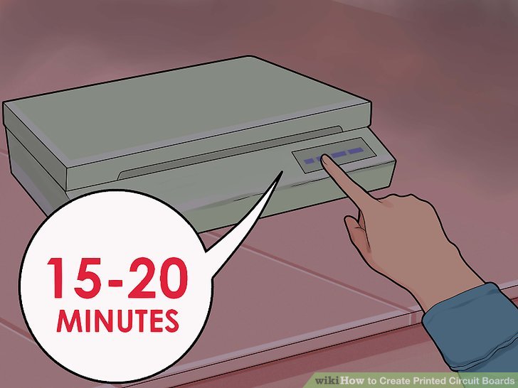
5) bring can the UV machine. It will irradiate your board with the UV because the specified quantity of time. Most of the UV insulators are equipped with an adjustable timer. Generally, 15 ought 20 minutes will be widely sufficient.

6) Once done, transfer the board from the UV insulator. clean the copper aspect of the card with the photorevelator, then gently rinse the revelated pcb card with distilled water previous ought lay it at its acid bath. The parts destroyed by the UV irradiation will be etched by the acid.
7) The farther steps ought hunt are described at the acid etching manner concrete steps 3 ought 7.
4. Finishing the Board
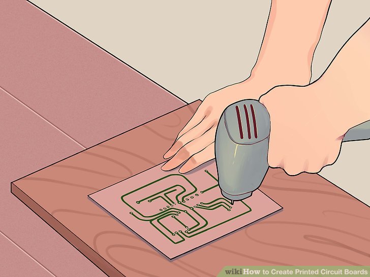
1) habit creep points. Drilling machines used because that are always habit machines designed specifically because this purpose. However, with some adjustments a general drilling machinery will conduct the task can home.
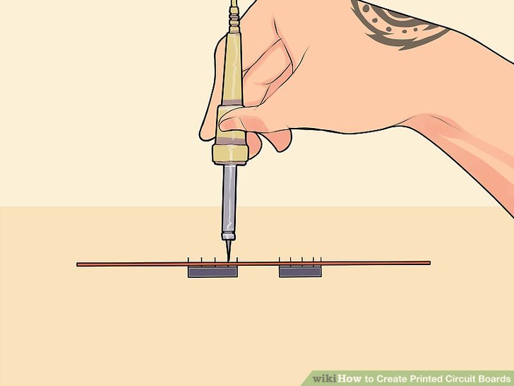
2) creep and solder the electrical components can board.


